Multi Channel Finite Impulse Filter Core
Overview
Finite Impulse Response (FIR) filters are important building blocks in signal processing.
beam processing, diffraction compensation, equalisation and various signal processing applications. Many applications often involve filtering multiple data channels simultaneously, raising concerns about resource utilization. This design implements a multi-channel FIR filter (MFF) which allows multiple FIR filters to use the same hardware in a sequential manner, optimizing resource utilization. This MFF is a viable solution particularly suited for scenarios characterized by low data rates relative to the system clock.
In this design, data and coefficient widths, number of data channels and filter taps are all user selectable. All FIR filters have an identical number of taps. Filter taps can have the same or different values. MFF output width, as well as internal multiplier output width are also user selectable. This allows the user to optimize the filter outputs and resource utilization.
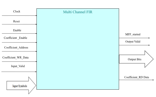
Coefficients can be written/read though a coefficient interface as shown below,
| Coefficient Interface Signals | |||
| Coef_En | Coefficient Enable | In | std_logic |
| Coef_We | Coefficient Write Enable | In | std_logic |
| Coef_Adr | Coefficient Address | In | std_logic_vector |
| Coef_Data_Wr | Coefficient write data | In | std_logic_vector |
| Coef_Data_Rd | Coefficient read data | Out | std_logic_vector |
The MFF is implemented using VHDL and capable of being used on any FPGA/ASIC architecture.
Features
- Multi Channel FIR filter
- Selectable data and coefficient widths
- Selectable number of data channels
- Selectable number of filter taps
- Selectable output width
- Selectable inner multiplier output width
- Resource sharing
- Fully synchronous design using only one clock
- Area/Power efficient RAM based architecture
- Coefficient read back available
- Low latency
- Multiple MFFs can be combined in parallel to form MFF banks
Deliverables
- Synthesizable RTL source code in VHDL
- Comprehensive verification test bench and vectors in VHDL
- Integration documentation and user guide
Performance
Maximum clock speed depends on the application process but typically is at least 160 MHz for a 65 nm ASIC process. Clock speeds of greater than 160 MHz have been achieved for FPGA.s i.e. Microsemi Polarfire. The resource utilization is given for 24 bit coefficient and input data, and 24 bits output, with 32 bits internal multiplier output.
| FPGA implementation (Polarfire FPGA MPF300T) | |||
| Number of FIR filters/ Number of Filter Taps | 64 | 128 | 256 |
| 16 | 170Mhz | 165Mhz | 160Mhz |
| 32 | 165Mhz | 160Mhz | 160 |
| FPGA implementation (Polarfire FPGA MPF300T) | |||
| Number of FIR filters/ Number of Filter Taps | 64 | 128 | 256 |
| 16 | 520 Dffs, 4 Dsp blocks, 81.5 kbits RAM | 524 Dffs, 4 Dsp blocks, 121.5 kbits RAM | 536 Dff, 4 Dsp blocks, 201.5 kbits RAM |
| 32 | 524 Dffs, 4 Dsp blocks, 121.5 kbits RAM | 536 Dff, 4 Dsp blocks, 201.5 kbits RAM | 541 Dff, 4 Dsp blocks, 481.5 kbits RAM |
Note 1: Clock Rate = 100 MHz
Specifications subject to change without notice. Information furnished by Paragon is believed to be accurate and reliable. However, no responsibility is assumed by Paragon for its use. All company and product names are trademarks or registered trademarks of their respective owners. All rights reserved. © 2011 Paragon Limited.